Tennant20 - Osmium coating: The way to go in SEM
New Osmium Coating System with Enhanced Features
Until now sputter coating is commonly used for SEM sample preparation, to coat non-conductive samples with a thin conductive layer. However, the grain size and directional coating in Sputter Coaters is not ideal. Osmium CVD-coating can overcome some physical problems sputter coating shows. The Tennant20 is expected to solve those problems.
As the osmium coating technology can be applied not only to SEM observation but also to other e-beam analysis techniques, such as elemental analysis, more than 400 osmium coating systems have been sold in Japan and are being used by users in various fields.
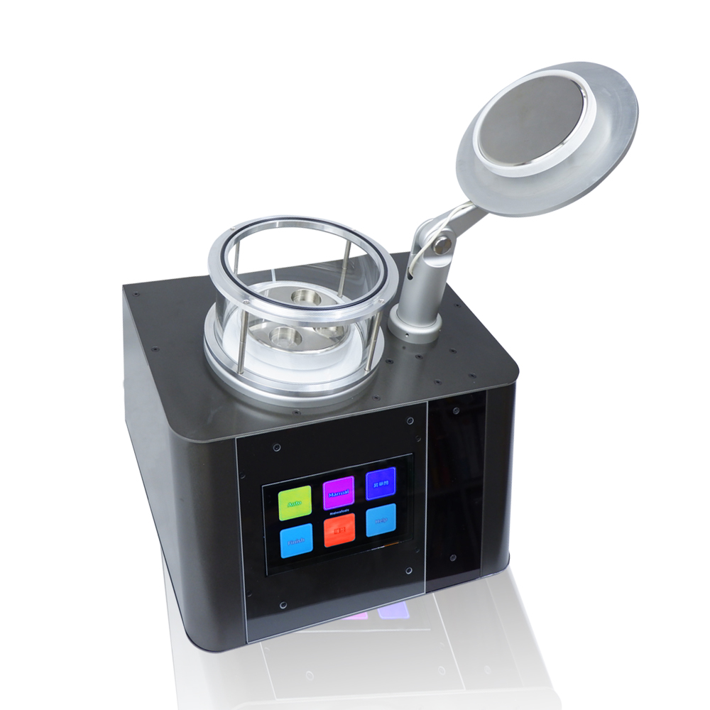 The Tennant20
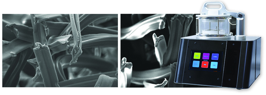
The Tennant20 Os-Coater is an advanced table-top PE-CVD system that creates high-quality pure conductive Os coatings for SEM sample preparation. The rotary pumped system creates ultra-thin coatings with very small grain-size and high conductivity.
Even on samples with a complicated structure, an Os film of 1-3nm thickness fully coats every side of the sample yielding very low charging effects in the SEM. Ultra-thin coatings <1nm show very small signal in EDX, AES, XPS, EBSD analysis.
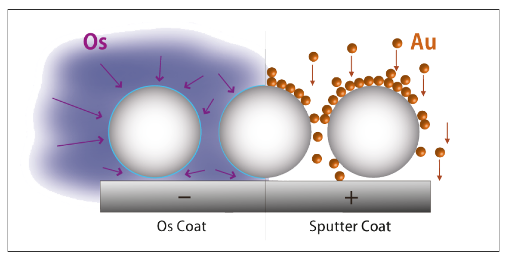
Os PE-CVD Plasma coating vs. Au Sputter coating
The Plasma CVD Method
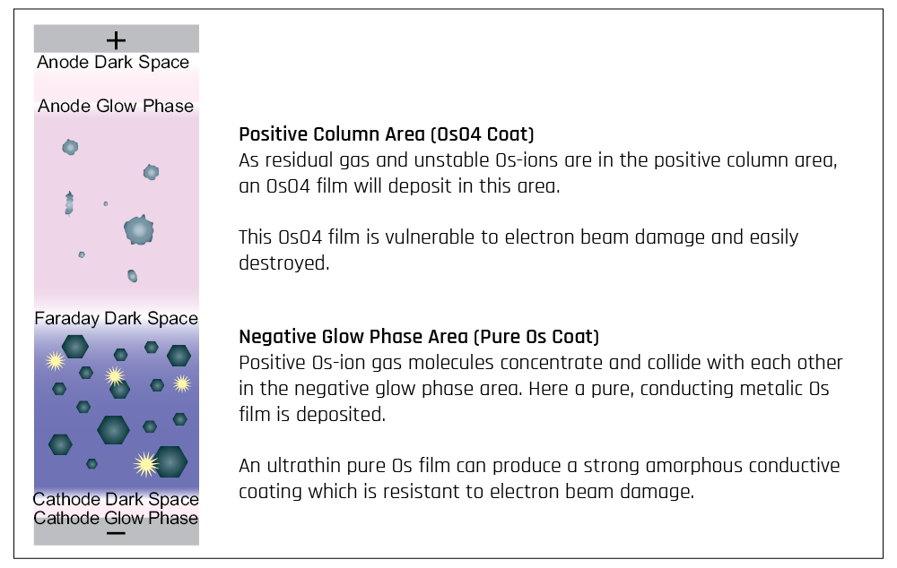
By the PE-CVD method, osmium tetroxide sublimation gas is introduced into the vacuum chamber, and plasma is generated by DC glow discharge.
The Tennant20 is feedback controlled to stabilize the coating current to realize highly reproducible film deposition. The coating current is measured every 1/10000s and analyzed by a 32-bit microprocessor. Based on PID control, the output of the discharge circuit is adjusted using a unique algorithm. During the procedure, the chamber is separated into two areas: „positive column“ and „negative glow phase.“
The negative glow phase area of conventional electrodes is only 5mm high. An OsO4 coat is formed in the positive column area if a sample is taller than 5mm. losing the original surface texture. The different appearence of the surface is visible even at a lower magnifications (see images SiC Wheel below).
Unlike conventional coaters the Tennant20 has special electrodes enabling a negative glow phase of up to 20mm.
SiC Wheel
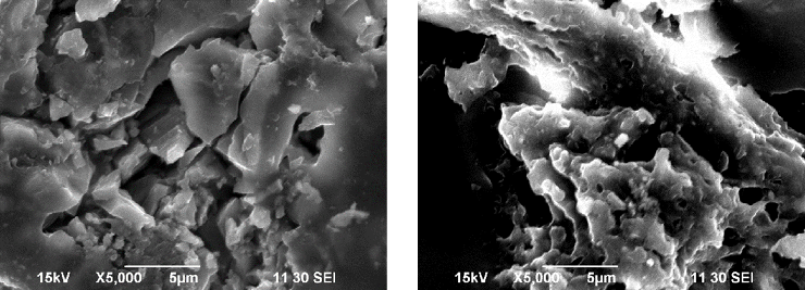
Left) Negative Glow Phase, Magnification : x5.000
Right) Positive Column, Magnification : x5.000
While the details can be observed without charge-up after the sample is coated in the negative glow phase, there is some charge-up in the sample coated in the positive column area as an OsO4 coat is susceptible to electron beam damage.
Acetate Fiber
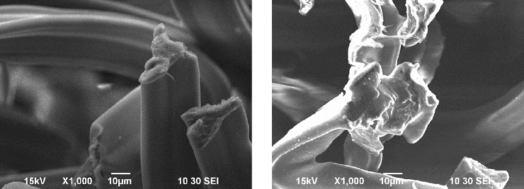
Left) Negative Glow Phase, Magnification : x1.000
Right) Positive Column, Magnification : x1.000
Even samples which are usually difficult to image, as they are easily affected by charging and drifting, Os coating provides a clear image when it is purely coated in the negative glow phase area in our Os coating system.
No Granularity At High Magnification
Polymer Film
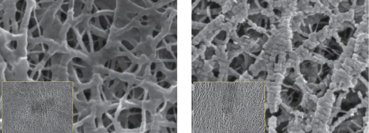
Left) OS coating, Magnification: x100.000
Right) Pt coating, Magnification: x100.000
A huge difference can be seen at a high magnification (x100,000). Pt has been sputtered on the sample and it is hard to see the original surface structure. No granularity is visible on the Os coated sample at a high magnification and you can see the actual surface structure. Also Os coating does not cause heat damage to organic samples due to the low landing energy.
Data provided by The Industrial Technology Research Institute (ITRI)
Related Products
-
 Art.Nr: MFTE20
The Tennant20 is an automated PE-CVD system for the production of ultra-thin coatings for SEM, EDX, EBSD, AES and XPS analyses. The rotation-pumped, closed system produces isotropic osmium layers with very small grain sizes and high conductivity. A large number of built-in safety functions ensure safe handling in accordance with laboratory standards.
Take advantage of our free coating service and experience this unknown but proven coating method. Detailed information can be found here.
-
Starting at €58.40 €69.50
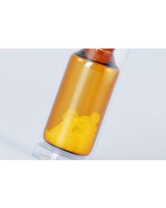
Small size (2ml), light-gauge, pre-scored amber glass ampoules. Ampoules containing OsO4 crystals are pre-cleaned and heat sealed in plastic bags to assure a contaminant-free solution.Starting at €58.40 €69.50
-

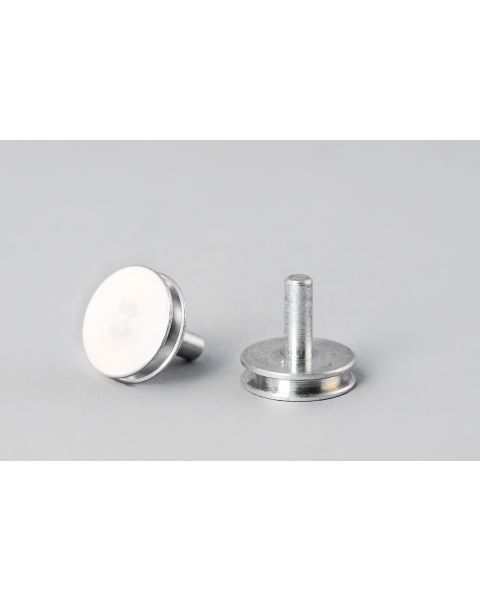
Starting at €3.40 €4.05
Made from pure aluminium. Lathe finish.Starting at €3.40 €4.05