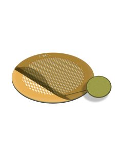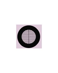
Continuous Silicon Nitride Film TEM Window Grids, square/slots
Silicon frames are 100µm thick. Grids fit standard 3mm holders and most double tilt holders.
Thicknesses available are 5, 10, 15, 20, 30, 50, 100 and 200 nm, window sizes are squares of 0,01mm, 0,025, 0,05, 0,1, 0,15, 0,25, 0,5, 1mm or arrays.
Product Details
Description
Features
- Plasma Cleanable - can be vigorously plasma cleaned to remove organic contamination
- High Temperature Tolerance - resist temperatures up to and above 1000°C
- Mechanical Robustness - withstand harsh conditions
- Flat, insulating and hydrophobic - incorporates LPCVD, low-stress(~250MPa), non-stoichiometric silicon nitride
- Chemically Inert - resistant to bases, acids (except HF) and solvents
- High Beam Current Tolerant
- Carbon-Free and Ultra-Clean
- Good X-ray transmission performance
- Compatible - fit standard 3mm TEM grid holders, octagonal shape
Uses:
- Environmental TEM (dynamic processes at high temperatures)
- Nanoparticle imaging
- Analysis of nano materials, semiconductor materials, optic-crystal materials, functional film materials etc.
- (Quantitative) Carbon Analysis (photoresist, polymers, food, oil, fuel etc.)
- Crystal growth research
- X-Ray microscopy and X-Ray spectroscopy techniques
- Thin film research
- In-situ characterization of chemical reactions and annealing effects
- Biological sample observation thanks to superior biocompatibility: on-film growth of cells or other biological samples
- Characterization experiments of colloids, aerogels, organic materials and nanoparticles
Recommended Use
| SiN film thickness | Product examples and window sizes | |
|
Highest Resolution Imaging |
5nm | E76042-43, 1 square (0,025mm) E76042-44, 8 squares (0,05mm), 1 slot (0,05x0,1mm) E76042-45, 2 slots (0,05x1,5mm)* |
| High Resolution | 10nm | E76042-46, 8 squares (0,1mm), 1 slot (0,1x0,35mm) E76042-47, 8 squares (0,25mm), 1 slot (0,25x0,5mm) YSG010Z, 1 square (0,1mm) YSG015Z, 1 square (0,15mm) YSG025Z, 1 square (0,25mm) YSG050Z, 1 square (0,5mm) YSAR010Z, 9 squares (0,1mm) |
| Everyday Imaging | 20nm | YSG001AT, 1 square (0,01mm) E76042-48, 8 squares (0,1mm), 1 slot (0,1x0,35mm) E76042-49, 1 square (0,5mm) E76042-50, 9 squares (0,1mm) |
| Demanding Conditions | 50nm | E76042-53, 1 square (0,1mm) E76042-52, 1 square (0,5mm) E76042-51, 1 square (1mm) YSTA015C, 2 slots (0,1x1,5mm) E76042-50, 9 squares (0,1mm) |
| Suspension Materials & Cryo-TEM | Microporös, nanoporös | E76042-41, 1 square (0,5mm) E76042-40, 1 square (0,5mm) YSME050B, 1 square (0,5mm), 2,8μm holes YSME050C, 1 square (0,5mm), 2,0μm holes YSME050C10, 1 square (0,5mm), 10μm holes YSME050E05, 1 square (0,5mm), 5μm holes YSNP-TE025B, 1 square (0,25mm), 20-200nm holes, 50nm SiN YSNP-TE010D, 1 square (0,1mm), 20-200nm holes, 200nm SiN |
*Coated with 1nm ultrahigh purity carbon to minimize charging
More Information
| Film Type |
Continuous SiN film
|
|---|---|
| Material |
Silicon Nitride
|
-
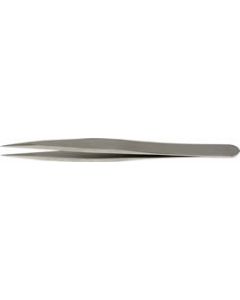
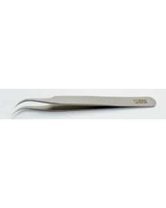
 €87.40 €104.01Art.Nr: E78322-7TEEMS Pinzette mit feinen, gebogenen Spitzen. Länge 115mm.€87.40 €104.01
 -
 €80.10 €95.32Art.Nr: E72919-2ATEEMS Tweezers with flat, PTFE coated tips. Provides a larger flat gripping surface for better handling of small objects without puncturing them (membrane, wafer etc.).€80.10 €95.32
 -
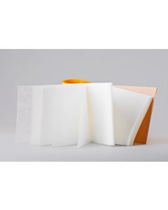 €8.60 €10.23Art.Nr: E71712-01EMS Lens Tissue is the world's finest optical tissue. It's extremely soft and virtually lint-free. Safe for any optical surface such as camera lenses, microscopes, telescopes, and eye-glasses. Each tissue is perforated for easy removal from the booklet.€8.60 €10.23
 -
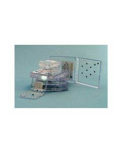
Starting at €589.40 €701.39
Gel-coating keeps devices in place, even if container is tilted or jarred. Ideal for handling subassemblies, hybrid models and packaged devices.Starting at €589.40 €701.39
-
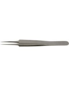 €86.50 €102.94Art.Nr: E0304-5-TFDumont Tweezer with fine, strong and Teflon coated points. Tip measures: A: 0,06mm B: 0,10mm. Length: 110mm€86.50 €102.94
 -

Starting at €27.30 €32.49
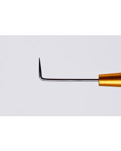
Rubis Plastic Tweezers with fine, strong hook tips. Length 120mm.Starting at €27.30 €32.49
-
Starting at €54.90 €65.33
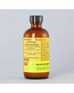
Glass distilled acetone is a high purity solvent. During manufacture, it only comes into contact with glass appliances. Glass distilled Acetone is used for dehydration, fixation and during infiltration in electron microscopy.
Starting at €54.90 €65.33


Downloads

Who Viewed This Also Viewed