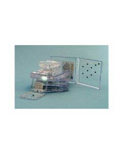
Microporous Silicon Nitride Film TEM Window Grids
Microporous SiN TEM Windows offer a range of different pore sizes (2-10 μm) on a square silicon nitride membrane. This enables observation in the TEM without background noise. SiN film thicknesses of 20, 30, 50 or 200nm available.
Product Details
Description
Features
- Plasma Cleanable - can be vigorously plasma cleaned to remove organic contamination
- High Temperature Tolerance - resist temperatures up to and above 1000°C
- Mechanical Robustness - withstand harsh conditions
- Flat, insulating and hydrophobic - incorporates LPCVD, low-stress(~250MPa), non-stoichiometric silicon nitride
- Chemically Inert - resistant to bases, acids (except HF) and solvents
- High Beam Current Tolerant
- Carbon-Free and Ultra-Clean
- Good X-ray transmission performance
- Compatible - fit standard 3mm TEM grid holders, octagonal shape
Uses:
- Environmental TEM (dynamic processes at high temperatures)
- Nanoparticle imaging
- Analysis of nano materials, semiconductor materials, optic-crystal materials, functional film materials etc.
- (Quantitative) Carbon Analysis (photoresist, polymers, food, oil, fuel etc.)
- Crystal growth research
- X-Ray microscopy and X-Ray spectroscopy techniques
- Thin film research
- In-situ characterization of chemical reactions and annealing effects
- Biological sample observation thanks to superior biocompatibility: on-film growth of cells or other biological samples
- Characterization experiments of colloids, aerogels, organic materials and nanoparticles
Recommended Use
| SiN film thickness | Product examples and window sizes | |
|
Highest Resolution Imaging |
5nm | E76042-43, 1 square (0,025mm) E76042-44, 8 squares (0,05mm), 1 slot (0,05x0,1mm) E76042-45, 2 slots (0,05x1,5mm)* |
| High Resolution | 10nm | E76042-46, 8 squares (0,1mm), 1 slot (0,1x0,35mm) E76042-47, 8 squares (0,25mm), 1 slot (0,25x0,5mm) YSG010Z, 1 square (0,1mm) YSG015Z, 1 square (0,15mm) YSG025Z, 1 square (0,25mm) YSG050Z, 1 square (0,5mm) YSAR010Z, 9 squares (0,1mm) |
| Everyday Imaging | 20nm | YSG001AT, 1 square (0,01mm) E76042-48, 8 squares (0,1mm), 1 slot (0,1x0,35mm) E76042-49, 1 square (0,5mm) E76042-50, 9 squares (0,1mm) |
| Demanding Conditions | 50nm | E76042-53, 1 square (0,1mm) E76042-52, 1 square (0,5mm) E76042-51, 1 square (1mm) YSTA015C, 2 slots (0,1x1,5mm) E76042-50, 9 squares (0,1mm) |
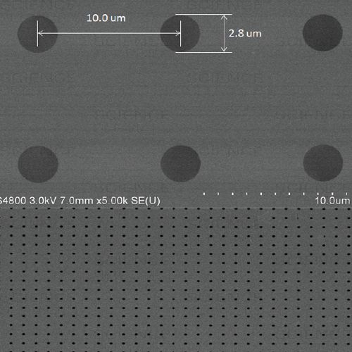
| Suspension Materials & Cryo-TEM | Microporös, nanoporös | E76042-41, 1 square (0,5mm) E76042-40, 1 square (0,5mm) YSME050B, 1 square (0,5mm), 2,8μm holes YSME050C, 1 square (0,5mm), 2,0μm holes YSME050C10, 1 square (0,5mm), 10μm holes YSME050E05, 1 square (0,5mm), 5μm holes YSNP-TE025B, 1 square (0,25mm), 20-200nm holes, 50nm SiN YSNP-TE010D, 1 square (0,1mm), 20-200nm holes, 200nm SiN |
*Coated with 1nm ultrahigh purity carbon to minimize charging
More Information
| Film Type |
Mikroporous SiN film
|
|---|---|
| Material |
Silicon Nitride
|
-
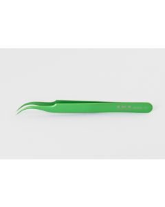 €87.40 €104.01Art.Nr: E78322-7TEEMS Pinzette mit feinen, gebogenen Spitzen. Länge 115mm.€87.40 €104.01
 -
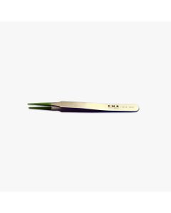 €80.10 €95.32Art.Nr: E72919-2ATEEMS Tweezers with flat, PTFE coated tips. Provides a larger flat gripping surface for better handling of small objects without puncturing them (membrane, wafer etc.).€80.10 €95.32
 -
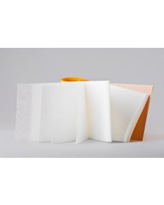 €8.60 €10.23Art.Nr: E71712-01EMS Lens Tissue is the world's finest optical tissue. It's extremely soft and virtually lint-free. Safe for any optical surface such as camera lenses, microscopes, telescopes, and eye-glasses. Each tissue is perforated for easy removal from the booklet.€8.60 €10.23
 -
Starting at €589.40 €701.39
Gel-coating keeps devices in place, even if container is tilted or jarred. Ideal for handling subassemblies, hybrid models and packaged devices.Starting at €589.40 €701.39
-
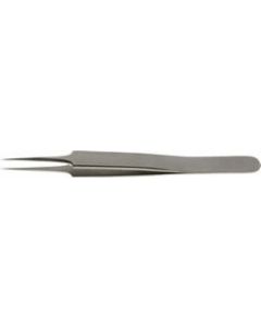 €86.50 €102.94Art.Nr: E0304-5-TFDumont Tweezer with fine, strong and Teflon coated points. Tip measures: A: 0,06mm B: 0,10mm. Length: 110mm€86.50 €102.94
 -

Starting at €27.30 €32.49
Rubis Plastic Tweezers with fine, strong hook tips. Length 120mm.Starting at €27.30 €32.49
-
Starting at €54.90 €65.33
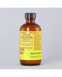
Glass distilled acetone is a high purity solvent. During manufacture, it only comes into contact with glass appliances. Glass distilled Acetone is used for dehydration, fixation and during infiltration in electron microscopy.
Starting at €54.90 €65.33


Downloads

Who Viewed This Also Viewed