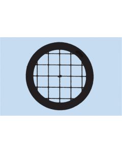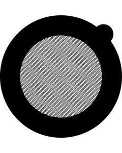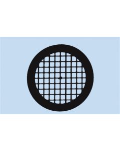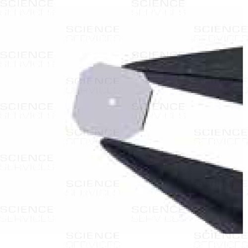
Nanoporous Silicon Nitride Film TEM Window Grids
Nanoporous SiN TEM Windows feature a range of different pore sizes (20-200nm) on a square silicon nitride membrane. This enables observation in the TEM without background noise. SiN film thicknesses of 15, 20, 30, 50, 100 or 200nm available.
Product Details
Description
Eigenschaften:
- Plasmareinigung möglich - Entfernung von organischen Verunreinigungen
- Hochhitzebeständig - bis zu 1000°C und mehr
- Mechanische Robustheit - halten auch anspruchsvollen experimentellen Bedingungen stand
- Flach, isolierend und hydrophob - LPCVD, „low-stress“ SiN (<250MPa), nicht-kristallines SiN mit <0,5nm Rauigkeit
- Chemisch inert - beständig gegenüber Säuren (mit Ausnahme von HF), Basen und Lösungsmitteln
- Resistent gegen hohe Strahlstromstärken
- Kohlenstofffrei und ultra-rein
- Gute Röntgen- und e-Strahl-Transmission
- Kompatibel – passen in normale 3mm TEM-Probenhalter, achteckig (daher auch gut mit der Pinzette aufnehmbar)
- Homogen – <0,5nm Variation in der Filmdicke nicht nur im einzelnen Grid sondern über eine komplette Produktions-Log hinweg
Anwendungsgebiete:
- Environmental TEM (dynamische Prozesse bei hohen Temperaturen)
- Nanopartikel-Untersuchung
- Charakterisierung von Materialien aus den Bereichen Nano, Halbleiter, optische Kristalle, funktionale Materialien u.v.m.
- (Quantitative) Kohlenstoff-Analyse (z.B. Fotolack, Polymere, Nahrung, Öl, Kraftstoffe)
- Kristallzüchtung
- Röntgen-Mikroskopie and Röntgen-Spektroskopie
- Dünnfilm-Forschung
- In-situ-Charakterisierung von chemischen Reaktionen und Temper-Effekten
- Beobachtung biologischer Systeme durch gute Biokompatibilität: Wachstum von Zellen oder anderen biologischen Einheiten direkt auf dem Film
- Charakterisierung von Kolloiden, Aerogelen, organischen Materialien, Halbleitern, Kristallen und Nanopartikeln
Empfohlene Anwendunge
|
|
SiN Film-Dicke |
Produktbeispiele und Fenstergröße |
|
Höchstauflösung |
5nm |
E76042-43, 1 Quadrat (0,025mm) E76042-44, 8 Quadrate (0,05mm), 1 Slot (0,05x0,1mm) E76042-45, 2 Slots (0,05x1,5mm)*
|
|
Hohe Auflösung |
10nm |
E76042-46, 8 Quadrate (0,1mm), 1 Slot (0,1x0,35mm) E76042-47, 8 Quadrate (0,25mm), 1 Slot (0,25x0,5mm) YSG010Z, 1 Quadrat (0,1mm) YSG015Z, 1 Quadrat (0,15mm) YSG025Z, 1 Quadrat (0,25mm) YSG050Z, 1 Quadrat (0,5mm) YSAR010Z, 9 Quadrate (0,1mm)
|
|
Routine |
20nm |
YSG001AT, 1 Quadrat (0,01mm) E76042-48, 8 Quadrate (0,1mm), 1 Slot (0,1x0,35mm) E76042-49, 1 Quadrat (0,5mm) E76042-50, 9 Quadrate (0,1mm)
|
|
Herausfordernde Bedingungen |
50nm |
E76042-53, 1 Quadrat (0,1mm) E76042-52, 1 Quadrat (0,5mm) E76042-51, 1 Quadrat (1mm) YSTA015C, 2 Slots (0,1x1.5mm) E76042-50, 9 Quadrate (0,1mm)
|
|
Materialien in Lösung & Cryo-TEM |
Microporös, nanoporös |
E76042-41, 1 Quadrat (0,5mm) E76042-40, 1 Quadrat (0,5mm) YSME050B, 1 Quadrat (0,5mm), 2,8μm Löcher YSME050C, 1 Quadrat (0,5mm), 2,0μm Löcher YSME050C10, 1 Quadrat (0,5mm), 10μm Löcher YSME050E05, 1 Quadrat (0,5mm), 5μm Löcher YSNP-TE025B, 1 Quadrat (0,25mm), 20-200nm Löcher, 50nm SiN YSNP-TE010D, 1 Quadrat (0,1mm), 20-200nm Löcher, 200nm SiN u.v.m. |
* beschichtet mit 1nm ultrareinem Kohlenstoff, um Aufladung zu minimieren
More Information
| Film Type |
Nanoporous SiN film
|
|---|---|
| Material |
Silicon Nitride
|
-
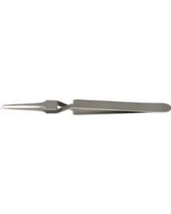
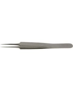
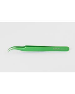 €87.40 €104.01Art.Nr: E78322-7TEEMS Pinzette mit feinen, gebogenen Spitzen. Länge 115mm.€87.40 €104.01
 -
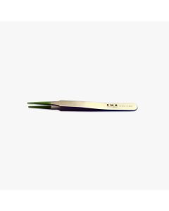 €80.10 €95.32Art.Nr: E72919-2ATEEMS Tweezers with flat, PTFE coated tips. Provides a larger flat gripping surface for better handling of small objects without puncturing them (membrane, wafer etc.).€80.10 €95.32
 -
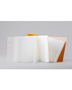 €8.60 €10.23Art.Nr: E71712-01EMS Lens Tissue is the world's finest optical tissue. It's extremely soft and virtually lint-free. Safe for any optical surface such as camera lenses, microscopes, telescopes, and eye-glasses. Each tissue is perforated for easy removal from the booklet.€8.60 €10.23
 -
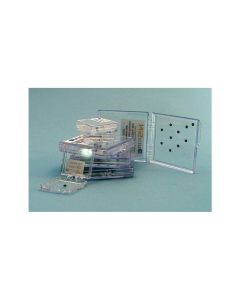
Starting at €589.40 €701.39
Gel-coating keeps devices in place, even if container is tilted or jarred. Ideal for handling subassemblies, hybrid models and packaged devices.Starting at €589.40 €701.39
-
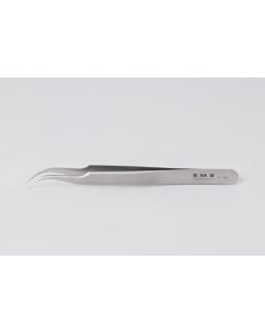
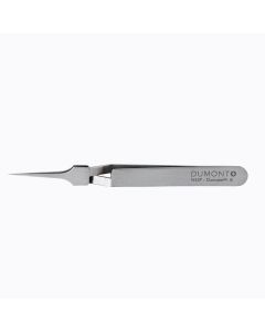
 €86.50 €102.94Art.Nr: E0304-5-TFDumont Tweezer with fine, strong and Teflon coated points. Tip measures: A: 0,06mm B: 0,10mm. Length: 110mm€86.50 €102.94
 -

Starting at €27.30 €32.49
Rubis Plastic Tweezers with fine, strong hook tips. Length 120mm.Starting at €27.30 €32.49
-
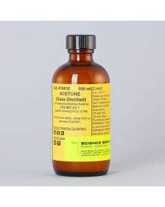
Starting at €54.90 €65.33
Glass distilled acetone is a high purity solvent. During manufacture, it only comes into contact with glass appliances. Glass distilled Acetone is used for dehydration, fixation and during infiltration in electron microscopy.
Starting at €54.90 €65.33


Downloads

Who Viewed This Also Viewed