Wafer
(9)The silicon wafer - a product from the semiconductor industry - is also a proven substrate in microscopy. Due to the controllable conductivity and the defined flat and very smooth surface, silicon wafers are ideal as a substrate or sample carrier for various types of sample material.
Please find more information about wafers below the products.
-
Starting at
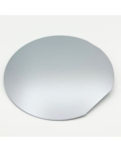
The silicon wafer have a diameter of 100mm and have the following approximate properties:
Type: n / Phosphor; Orientation: (100); Thickness: app. 525µm, Resistance: <10 Ohmcm. Depending on the batch thickness or resistance may vary slightly. The wafers are polished on one side. Wafer carrier/box included (no clean room quality).Starting at
-

Starting at
The silicon wafer have a diameter of 100mm and have the following approximate properties:
Doping: boron (p type); Orientation: (100); Thickness: app. 525µm, Resistance: <20 Ohmcm. Depending on the batch thickness or resistance may vary slightly. The wafers are polished on one side. Wafer carrier/box included (no clean room quality).Starting at
-
 €56.00 €66.64Art.Nr: MN7646
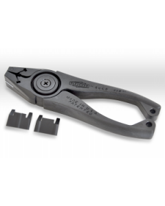
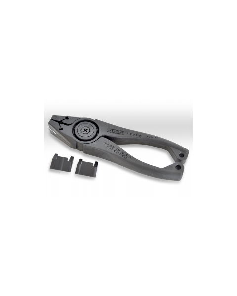
The CleanBreak wafer pliers are a simple and clean way to cleave (post scribe) wafers, wafer strips and smaller pieces down to 3cm. They are 15cm long and have a jaw opening of 1,9 cm. The CleanBreak pliers come with two sets of replaceable jaws to cleave crystalline or amorphous materials.
To cleave smaller pieces than 30mm we recommend the Small Sample Cleaving Pliers.
€56.00 €66.64 -
Starting at €13.00 €15.47
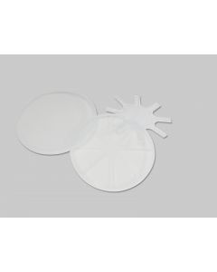
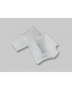
Transport containers for single 100mm wafers or other flat round substrates of similar size. The three-part transparent shells are made of antistatic polycarbonate. The star-shaped insert ensures that the wafer is held at the edges only.Starting at €13.00 €15.47
-
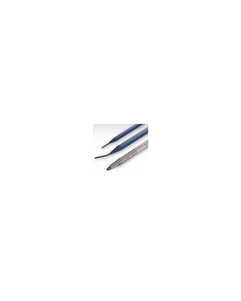
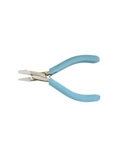 €65.70 €78.18Art.Nr: E7647The Small Sample Cleaving Pliers cleave samples into pieces from 1 - 30mm. Nylon jaws prevent sample damage and the included scribe alignment indicators increase the accuracy of cleaving. The double leaf spring at the fulcrum and plastic covered stainless-steel handles ensure easy handling and a comfortable grip.€65.70 €78.18
 -
 €21.00 €24.99Art.Nr: SC4T25The box is made of plastic and suitable for transporting 100mm (4") wafers. The sensitive wafers are protected against contamination and damage. The box is designed for the transport of up to 25 wafers 25.€21.00 €24.99
 -

Starting at €435.80 €518.60
A complete set of tools for clean cleaving of wafers into strips and small pieces. With this set good cut cross-sections are achieved. The Wafer Cleaving Kit Standard consists of three diamond scribers, tweezers, a small and large (optional) cutting mat and a pair of pliers.
Starting at €435.80 €518.60
-

Starting at €844.30 €1,004.72
The Wafer Cleaving Kit XL contains all components of the Wafer Cleaving Kit Standard (E7642) and in addition a premium quality diamond scriber and a pair of small sample cleaving pliers.
Starting at €844.30 €1,004.72
-
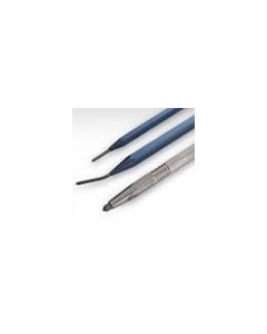 €194.10 €230.98Art.Nr: E7644The basic tools for wafer scribing. The Marker-Scriber Kit includes three diamond scribers for placing fine marks and scribing the wafer surface. These diamond scribers are also the replacements for those in the Wafer Cleaving Kit and XL (E7642, E7648).€194.10 €230.98


The silicon wafer - a product from the semiconductor industry - is also a proven substrate in microscopy. Due to the controllable conductivity and the defined flat and very smooth surface, silicon wafers are ideal as a substrate or sample carrier for various types of sample material.
Wafers are used in "non-transmissive" types of microscopy, such as scanning electron microscopy (SEM, FIB-SEM), atomic force microscopy (AFM, SPM), scanning tunnelling microscopy (STM) and reflected light microscopy.
The further development of the research field of scanning electron microscopy for 3D reconstruction of tissue with ultrastructural resolution, known as array tomography (AT), has opened up a new field of application for silicon wafers. Wafers are used as a substrate for the ATUMtome, a new type of ultramicrotome with an automatic section collector for series of ultra-thin sections. The sections obtained are collected on a carrier tape. After cutting, wafers are loaded with the tape. This creates so-called wafer libraries in which the series of sections can be stored and used for subsequent data acquisition. Smaller slice series can be collected with the ASH2 (Advanced Substrate Holder) on wafer pieces and ITO-coated cover glasses.
Science Services has added silicon wafers and the corresponding accessories, such as transport boxes and tools for dicing wafers, to its product range and is continuously expanding it to meet your requirements.
Of course, we also offer wafers for applications in micro- and nanotechnology in small to medium batches.
We have access to a large portfolio of our suppliers from Germany, Asia and the USA. From this we can supply wafers and chips made of silicon (Si), gallium nitride (GaN), gallium arsenide (GaAs), indium phosphide (InP), silicon carbide (SiC), aluminium nitride (AlN), lithium niobate (LiNbO3 / LN), sapphire, glass and quartz with different specifications.
Please contact us with your requirements.
We will be happy to answer your questions about technical properties and correct handling.